
EOS Drucker Service Pakete
Genau auf Ihre Bedürfnisse beim 3D-Druck zugeschnitten
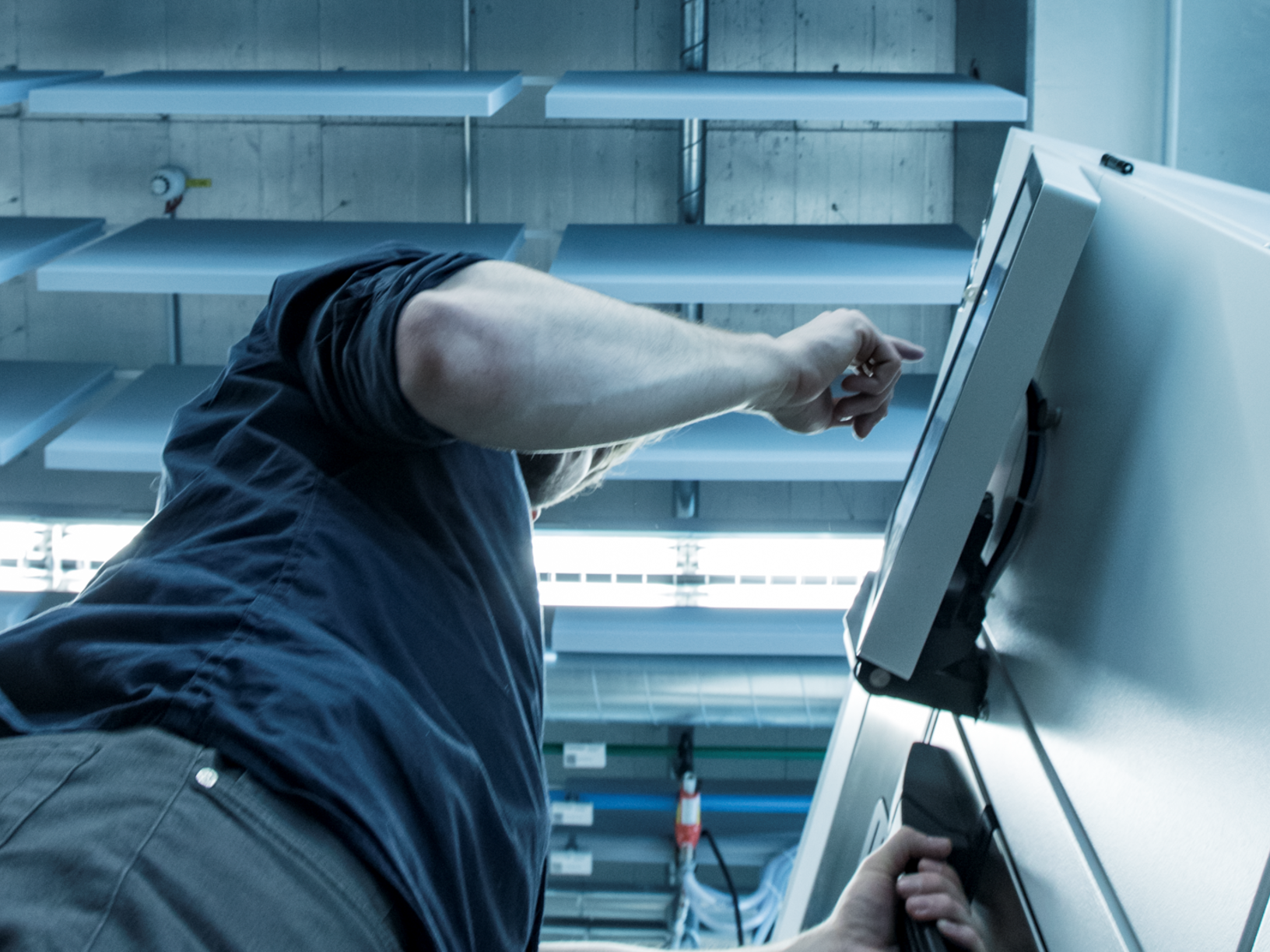
Von flexiblen Full-Service-Plänen bis zur Basispflege mit routinemäßigem Wartungscheck. Unser EOS System Care Programm ist auf Ihre spezifischen Anforderungen zugeschnitten. Wählen Sie einfach das richtige Paket für Ihre Lösungen und Ihren Servicebedarf.
Ihre Vorteile mit dem EOS System Care Programm
- Zugang zum EOS Service-Know-how
- Qualifizierte Anlagenwartung zur Sicherung des Werterhalts Ihres Anlagenparks
- Geringerer Bedarf an Druckerreparaturen und verbesserte Optimierung des Systemstatus
- Preisvorteile bei Servicetarifen
- Kostentransparenz und vorhersehbare Betriebskosten
EOS-Servicepakete für maximale Druckerverfügbarkeit und hochwertige Leistung
Mehr als ein einfacher Druckerreparaturservice: Wählen Sie die richtige Option für Ihre Installation!
Unsere flexiblen Servicepakete auf einen Blick
-
Download eos_system_care_program_flyer_de_web.pdf
EOS-Systempflegeprogramm
PDF 171,79 kB
Fernwartung durch EOS
Erhöhen Sie Ihre Systemverfügbarkeit mit Fernsupport auf ein Maximum
Sparen Sie Zeit und Geld mit EOS Remote Services. Unsere geschulten EOS Global Service Experten stehen Ihnen buchstäblich nur einen Mausklick entfernt zur Seite. Der Fernsupport verkürzt ungeplante Systemausfallzeiten und ermöglicht eine sichere Erstdiagnose sowie eine schnelle und sichere Störungsbehebung.
Sorgen Sie sich, wer Zugang erhält? Nicht mit EOS.
Unsere Lösung ist TÜV IT Trusted Product zertifiziert mit sicherer VPN-Verbindung, SSL-Verschlüsselung und Kommunikation über einen zentralen Server in einer DMZ (DeMilitarizedZone) - und Made in Germany.
Sie sind immer auf dem Fahrersitz: Die Verbindung zu Ihrem System ist nur möglich, wenn Sie sie initiieren. Sobald die Arbeit erledigt ist, wird die Remote-Sitzung geschlossen. Danach gibt es für EOS keine Möglichkeit, die Verbindung mit dem System wiederherzustellen - nur wenn Sie eine neue Fernwartungsanforderung starten. Sie brauchen sich also keine Sorgen zu machen, wenn Sie Ihren EOS Service-Experten direkt an Ihrer Seite haben.
Während der Garantiezeit und mit einem FullServiceFlex Servicepaket ist der Fernservice kostenlos.

Mehr erfahren
Von EOS Services Lösung
EOS Drucker Service Pakete
Von flexiblen Full-Service- und Wartungspaketen bis hin zur Basispflege mit einem System Health Check. Unsere Servicepakete sind individuell auf Ihre Bedürfnisse zugeschnitten.

EOS Finanzdienstleistungen
Für Ihren Erfolg mit additiver Fertigung Refurbished-Gebrauchtsysteme, flexible Leasing- und Finanzierungsmodelle: Mit unseren speziellen Angeboten ermöglichen wir Ihnen den Einstieg in den Ausbau Ihrer additiven Fertigung.

