Driving Down Cost of Ownership
EOS Nickel NiCP Pure Nickel for Advanced Semiconductor Applications
May 13, 2025 | Reading time: 5 min
Semiconductor equipment engineers and manufacturing specialists face unrelenting pressure to maximize wafer throughput while maintaining nanometer-level precision in chemically aggressive environments. Critical components in these systems require materials that deliver exceptional corrosion resistance without compromising performance or system uptime.
According to industry research published in 2024, corrosion in semiconductor manufacturing environments is responsible for over 50% of microelectronic device failures, representing a substantial impact on production efficiency and reliability.
EOS is partnering with global leading suppliers to address these challenges by offering a material innovation: EOS Nickel NiCP, a commercially pure nickel alloy with a minimum purity of 99.0%. This additive manufacturing (AM) material transforms how semiconductor manufacturers approach component design and production, eliminating traditional limitations of protective plating while enhancing component longevity.
Meeting the Demanding Requirements of Semiconductor Manufacturing
Semiconductor production operates at the extremes of precision. Temperature control within milliKelvin ranges is essential, as even minor thermal fluctuations can impact processes at the nanometer scale. Additionally, the industry's chemically aggressive environments present significant corrosion challenges for critical components.
Traditionally, manufacturers have relied on electroless nickel plating to protect chamber components from the harsh chemical environment of plasma chambers. While effective, this approach comes with limitations: First off, the protection layer has a finite lifespan, leading to increased consumable replacement and system downtime. In addition, plating processes can generate hazardous waste, including heavy metals and toxic chemicals.
With certain gasses commonly used in semiconductor manufacturing being heavily restricted, sustainable alternatives to traditional materials will be more and more important. Industries in the EU are setting the goal of 20% of global production by 2030, whereas the US Toxic Substances Control Act regulates restrictions on substances used in manufacturing. In the APAC region, major players like China, Singapore, Japan, and Hong Kong have announced plans to implement mandatory climate disclosures aligned with either the Task Force on Climate-Related Financial Disclosures or the International Sustainable Standards Board.

EOS Nickel NiCP: Pure Nickel Excellence Through Additive Manufacturing
EOS Nickel NiCP represents a breakthrough solution for these challenges. With a minimum nickel purity of 99.0%, this material meets the chemical composition requirements of ASTM B162 and SAE AMS5553, ensuring exceptional consistency and reliability for the most demanding applications.
Sourcing pure nickel billet through conventional methods can be difficult and costly, limiting its accessibility for high-performance manufacturing. The real innovation with EOS Nickel NiCP lies in how it transforms this limitation. Rather than applying protective plating to components, manufacturers can now build parts entirely from commercially pure nickel using AM technology. This approach eliminates the need for environmentally problematic plating processes while extending component lifespan and enhancing performance.

Key Benefits of EOS Nickel NiCP for Semiconductor Applications
- Enhanced corrosion resistance: With its exceptional purity, NiCP delivers outstanding resistance to corrosive environments directly impacting consumable lifetime, making it ideal for semiconductor chamber components and chemical processing equipment.
- Maximizing system uptime: Components built with NiCP can offer extended operational life compared to traditional plated parts. This maximizes equipment availability and increases overall wafer fabrication throughput — directly impacting manufacturers' bottom line.
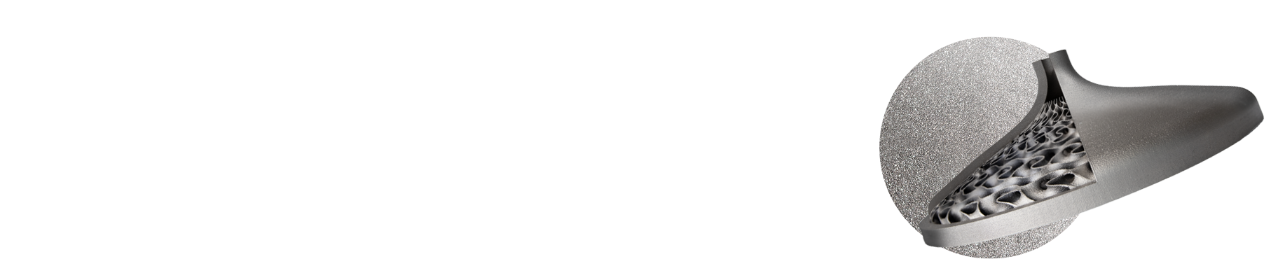
- Design optimization: AM with NiCP enables the creation of optimized thermal management solutions through complex internal channels and innovative geometries impossible with conventional manufacturing methods. These designs can significantly improve heat dissipation, system speed and accuracy.
- Reduced environmental impact: By eliminating the need for electroplating processes, NiCP offers a cleaner, more sustainable manufacturing approach that reduces hazardous waste generation while maintaining or improving component performance.
- Low stress characteristics: NiCP exhibits very low residual stresses, with parts that can often be used in the as-built state.
- Versatile manufacturing options: The material has been thoroughly tested across EOS' industrial 3D printing systems, including the M 290 and M 400-4. The 80 μm parameters on the M 400-4 enable exceptionally high build rates for production efficiency.
Beyond Semiconductors: Versatility Across Industries
While particularly well-suited for semiconductor applications, EOS Nickel NiCP's exceptional properties make it valuable for numerous other industries. Its excellent corrosion resistance and high purity make it ideal for chemical processing equipment and various applications requiring exposure to caustic environments.
The material's high ductility combined with good corrosion resistance opens possibilities for parts that must withstand both mechanical stress and chemical exposure — a common requirement in advanced industrial settings.
Transforming Manufacturing Through Material Innovation
EOS Nickel NiCP exemplifies how advanced materials combined with AM can solve long standing industrial challenges. By enabling the direct production of pure nickel components with optimized designs, EOS is helping semiconductor manufacturers improve performance, reduce environmental impact, and ultimately enhance productivity.
For industries where material purity, corrosion resistance, and precision are non-negotiable requirements, EOS Nickel NiCP offers a forward-thinking solution that addresses current manufacturing limitations while opening new possibilities for component design and performance.
Get Inspired

Nickel Alloys
This material characteristics make it ideal for a wide range of applications, for example in gas turbines for both aerospace and energy industries, process industry, oil and gas, ship building.

EOS M 290
Mid-sized and multi-talented, the industry standard for qualified metal 3D printed parts: Robust system design and powerful 400-watt fiber laser deliver reliable, high performance, day in and day out.

A Beginner's Guide to AM
Additive Manufacturing Blog
Are you new to the exciting world of AM? We've put together a comprehensive but straightforward guide in this blog