
3D Printing for Semiconductors
Enabling High-Precision, High-Performance Components for Next-Gen Semiconductor Manufacturing
The semiconductor industry is entering a renewed growth cycle. Global chip sales are forecast to rebound to USD 588 billion in 2024, driven by the recovery of the memory market, rising demand in PCs and smartphones, and accelerating momentum from generative AI applications, according to Deloitte’s 2024 Semiconductor Industry Outlook.
Despite this renewed growth, manufacturing complexity and competitive pressure continue to intensify. Communication and computing applications alone represented 56% of global semiconductor sales, while memory - nearly one-quarter of the market - remains a major swing factor influencing production volume and equipment requirements. This volatility puts OEMs and fabs under increasing pressure to maximize wafer yield, improve temperature uniformity, shorten development cycles, and build more resilient supply chains.
This is where Industrial 3D Printing becomes a catalyst for innovation - unlocking performance and design capabilities that traditional manufacturing simply cannot achieve.
Advantages of Industrial 3D Printing for Semiconductor Applications
AM Applications in Wafer Fabrication Equipment
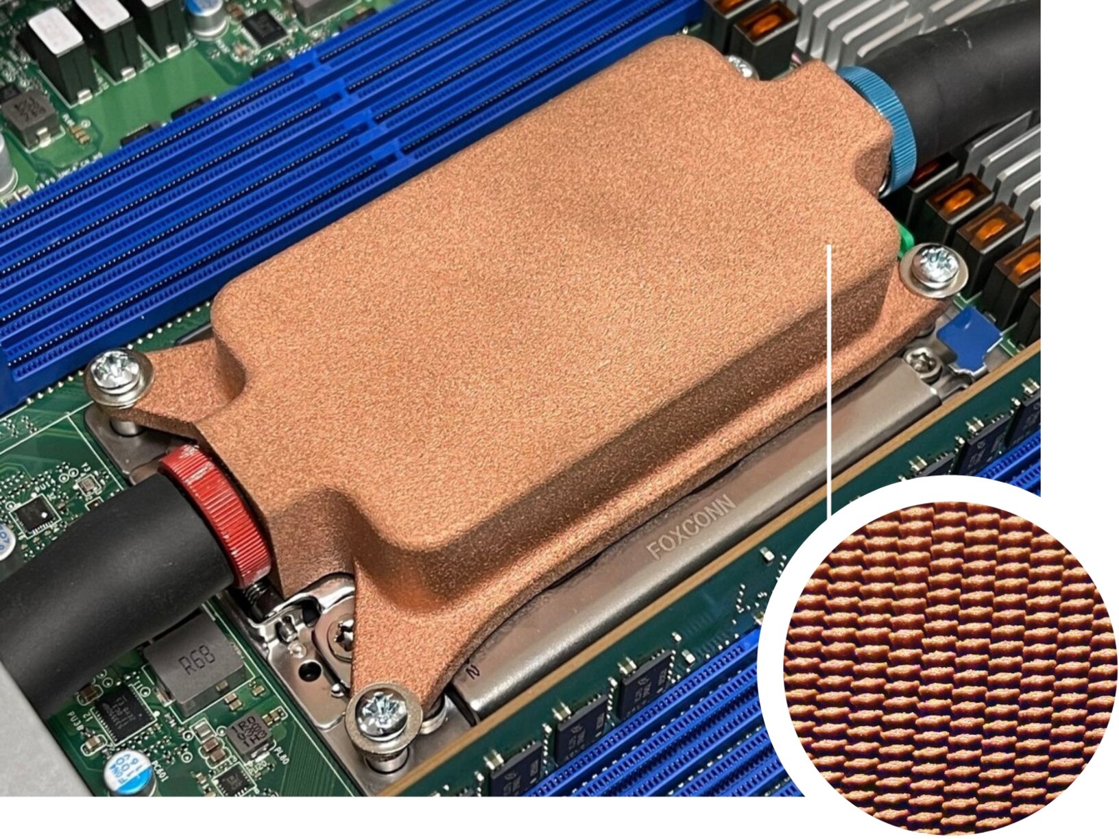
AM of Cooling Plates
Cooling plates are essential components within plasma chambers and wafer-processing submodules. Conventional production limits design complexity restricts thermal optimization and often involves long lead times. With AM, engineers can create conformal cooling channels that follow precise thermal profiles, improving backside wafer cooling and overall temperature uniformity.
By eliminating conventional machining constraints, AM enables larger channel diameters, increased cooling volume, optimized internal pathways, and faster iteration cycles. The result: improved yield, higher process stability, and reduced dependence on traditional supply chains.
HS Hitech
HS Hitech, a leading Korean semiconductor equipment parts supplier, partnered with EOS to overcome the limitations of a conventionally brazed cooling plate. The original design required complex assembly, risked leakage, and offered limited thermal efficiency and cooling surface. With EOS metal AM, the internal cooling architecture was completely re-engineered, achieving:
- +50% channel volume, +10% channel length
- +50% cooling surface area, +60% temperature uniformity
- –30% peak temperature
The AM-optimized part also showed reduced deformation in simulations and met all flow and pressure integrity requirements. This case demonstrates how additive manufacturing enables high-performance thermal components that significantly improve semiconductor process stability.

AM of Hydraulic Manifold & Power Systems
Wafer fabrication facilities rely on thousands of cooling, temperature-controlled and hydraulic power systems. These components must offer exceptional reliability and serviceability to minimize equipment downtime. Traditional manifolds, however, are limited in flow optimization, assembly complexity and long-term reliability. AM introduces new opportunities for OEMs and ODMs to customize and integrate thermal and hydraulic systems with improved flow mechanics, reduced assembly interfaces, and significantly enhanced durability.
HDC Co., Ltd.
HDC Co., Ltd. redesigned its hydraulic manifold system using EOS metal AM to overcome the limitations of conventional manufacturing. The AM manifold is 30% more compact and up to 70% lighter, with highly optimized curved internal flow paths that minimize pressure loss and eliminate the need for auxiliary caps and plugs.
By consolidating multiple parts into a single monolithic structure, the manifold becomes more robust, easier to maintain, and significantly more reliable. AM also enables full customization for modular equipment requirements, rapid lead times, and the integration of temperature or pressure sensors for predictive maintenance. This showcases how AM elevates hydraulic systems into high-performance, next-generation semiconductor components.

AM of Cooling Modules & Heat Sinks
AM unlocks entirely new design possibilities for heat exchangers, cooling modules, cold fingers and heat sinks. Engineers can integrate complex internal channel networks, lattice structures and high-surface-area geometries that dramatically enhance heat dissipation and cooling performance - far beyond what is possible through machining or brazing.
Delvy Oy
Delvy Oy demonstrated the transformative impact of AM by producing a copper heat exchanger with highly intricate internal channels and advanced lattice surfaces. Using EOS CuCP - a copper material with excellent thermal conductivity - the team achieved over 300% increase in dissipative surface area.
This enabled faster, more uniform temperature distribution, improved coolant circulation, reduced turbulence and more stable sensor temperatures in demanding semiconductor environments. The case exemplifies how AM can deliver unmatched thermal performance for next-generation cooling applications.


Shaping the Future of Semiconductor Thermal Management
Additive Manufacturing is already redefining how semiconductor equipment is designed, optimized and produced. Whether increasing cooling efficiency, improving temperature uniformity, reducing system footprint or enabling fully customized thermal architectures, EOS AM unlocks performance levels that traditional manufacturing cannot match. The examples highlighted here represent only the beginning.
Get Inspired


Additive Manufactured Heat Exchanger
Conflux | Success Story

3D Printing of Heat Exchanger
Applications
Industrial 3D printing enables ultra-efficient, compact heat exchangers with advanced internal geometries, faster development, and significant performance gains across electronics and thermal management applications.
Leak-Free, Liquid-Cooled Heat Sinks
CoolestDC | Success Story